You can see everything … except the data! Technical due diligence is a *must*.

You can see everything … except the data!  Technical due diligence is a *must*.
Holmes & Evans (source: NY Times)

I saw “You can see everything” with my wife on our date night last Friday. We both really liked it, and were puzzling away on the drive home about who said what to whom, who we thought was likely lying or truthful, what Elizabeth Holmes’ partner Bill Evans was really up to, whether Nathan Fielder (the journalist) was going to lunge and kiss Holmes (former CEO of Theranos) when she was hitting him with the puppy dog eyes, etc. We both knew of the events regarding Theranos generally, but were not well acquainted with the particulars prior to the movie, which probably made for better entertainment. 🙂

If you haven’t seen it yet, the movie is a meta-documentary that did a great job of immersing you in Holmes’ and Evans’ personal circumstances with their two young kids in the weeks prior to her having to report to prison in Texas in 2023 for defrauding investors out of hundreds of millions of dollars. It delves into Holmes’ and Evans’ claims of her innocence regarding her over-reaching/fraudulent statements about the company’s microfluidic blood analysis technology and its capabilities. SPOILER ALERT!! Fielder focussed on whether Holmes was intentionally deceiving people (i.e. investors, the public) when, in years past, she said things to the effect of ‘the product can do a multitude of tests simultaneously’. He was trying to determine whether she genuinely didn’t understand that this phrase would be interpreted by most to mean “the product has already successfully and conclusively demonstrated its ability to do a multitude of tests …”, not “the product can, in theory and once fully developed, do any and all of a multitude of tests …”. To get a better read on her interpretation of her own words, he gets her interpretation of the “Who’s on First” skit by Abbott and Costello, where her answers suggest that, by virtue of her very literal interpretation, she misses the double ententes that are the essence of the humour. They touch on whether she is neuro-divergent, and leave the audience to draw their own conclusions.
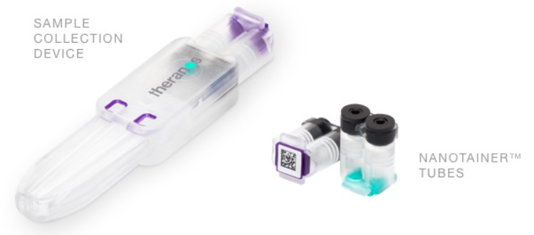
Theranos finger prick blood sampling device & sample tubes (source: Theranos.com via Wayback Machine)

The next morning, my wife and I were still sorting out all the loose ends during our dog walk. We discussed who we now believed to be truthful, and my wife was asking me about the microfluidics, analytical chemistry and business aspects of the story. This is also where my thoughts had led to, and is the reason I’m writing this article.

The short version of this post’s analysis can be summarised as follows: there’s no way the Theranos calamity would have happened had robust technical due diligence been performed. It can be put even more succinctly using the Russian proverb that the late President Reagan was fond of: trust, but verify.

As a microfluidics consultant who a) supports technology development projects, and b) performs technical due diligence investigations on behalf of prospective investors, I can tell you that I was dumbfounded as to how this situation could have arisen in the first place. While the trustworthiness of the leadership team at Theranos (or any company) would have been crucial to investor decision-making, so too should have been the imperative for, and results from, a rigorous technical due diligence investigation. My astonishment lead to a deeper dive into the events surrounding the rise and fall of Theranos, and especially into investment rounds that totalled over $900M USD from venture capitalists (VCs) and companies like Safeway and Walgreens.
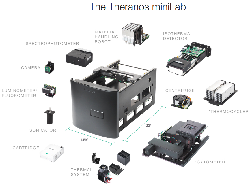
Theranos miniLab instrument (source: Theranos.com via Wayback Machine)

It turns out I’m very late to the party; much has been written on this very point. If you’re interested in the business and investment angle of the story, there is a pretty good Wikipedia entry for Theranos. and below are some references that explore various aspects of this story, including legal references, investigative journalism, an on-site interview video, and retrospective analyses and opinions on problems and failure modes.

  1. Wall Street Journal exposé on Thereanos’ inconsistent product performance, secrecy and fraudulent practices that kicked off the firestorm of trouble for the company (John Carreyrou, October 15th, 2015):
  2. Wall Street Journal exposé on Walgreens’ investment in Thereanos despite its misgivings due to secrecy regarding product performance (Christopher Weaver and John Carreyrou, May 25th, 2016):
    1. https://www.wsj.com/articles/craving-growth-walgreens-dismissed-its-doubts-about-theranos-1464207285
  3. CNN video tour of Theranos and interview with Holmes (Sanjay Gupta, August 1st, 2016):
  4. Editorial in the European Journal of Clinical Investigations criticising stealth (i.e. unpublished) research by start-up ‘unicorns’ (VC backed with valuations over USD $1B) (Ioana Cristea et al., April 1st, 2019):
  5. Editorial post mortem in the Journal of Medical Systems regarding the rise and fall of Theranos, highlighting steps such as encouraging engagement in academic collaborations, publication of scientific results, and revitalised investor due diligence (Rishub Das et al., April 4th, 2022)
  6. Lexology blog post regarding the importance of due diligence in light of Holmes’ fraud conviction (Ellen Lambrix, Bristows LLP, January 5th, 2022)
    1. https://www.lexology.com/library/detail.aspx?g=26af5d28-3c11-4440-880f-8806df327529
  7. Vaultinum blog post regarding Theranos’ secretive practices, unproven technology, and the importance of technical due diligence as an inoculant against future such travesties (Marine Yborra, May 18th, 2022)
  8. Legal summary for U.S. v. Elizabeth Holmes, et al., provided by the US Attorney’s Office, Norther California.

The answer to my question about how this could ever have come to be is essentially two-fold. Several top VC inventor firms refused to get involved when their attempts to perform technical due diligence were thwarted by Theranos’ insistence on secrecy, which they claimed was based on their need to protect their intellectual property (see reference 7). Other investors either didn’t bother trying to look that deeply, or weren’t willing to push Theranos to either a) expose its technology to scrutiny, or b) at least demonstrate product performance through independent testing against gold standard analytical methods. Walgreens investigative consultants were denied access and reported their reservations, but Walgreens persevered (see reference 2).

In the investment due diligence investigations I have performed, the start-ups have confidentially revealed all of their performance data, reports, and intellectual property (IP), and they have fully answered my innumerable questions about all aspects of their microfluidic devices, analytical instrumentation, protocols and procedures, and the performance achieved. This has allowed me in each case to write a detailed and accurate report for my client—the prospective investor—that fully described the extent to which IP, technology, performance, and the leadership team were evaluated, the findings in each of these areas, and my analysis and recommendations based on those findings. Some start-ups get rosier recommendations than others, naturally, but I have had full disclosure in all cases. Had I been met with resistance to supply information, I would have questioned the target company as to why, and then I would have clearly highlighted the resistance, missing information, and associated enormous risks in the report.

Thorough technical due diligence for investment in a deep tech-based company like Theranos should be regarded as mandatory by investors, not optional. I should note that I have not dealt with unicorn start-ups with their very aggressive growth curves, valuations, and leadership teams that are secretive about their technology. While I understand that a unicorn investment target represents a significant paradigm shift compared to a ‘normal’ start-up, and that a change in approach might be required for a technical due diligence investigation, the fundamental requirement of verifying product technology and performance must still be met. There really are no valid explanations or excuses that justify a lack of disclosure, or demonstration of performance; asking an investor to ‘take their word for it’ doesn’t pass muster. Suitable non-disclosure agreements (NDAs) can be used to safeguard the target company’s IP when revealed to the prospective investor or their consultant. Failing that, and at a minimum, performance comparisons against gold standard chemical analysis methods can still be demonstrated, even it the technology in question is treated as a secret black box to protect IP.

A lack of published results underpinning a technology does not prove the technology is faulty, but is a red flag, in my view. The increasing tendency of technology-based start-up unicorns to bypass the rigours of publishing their work in refereed journals is documented in references 4 and 5. Reluctance to publish is understandable in the context of a start-up with fast-approaching milestones and limited resources, as it is admittedly laborious and provides some level of potentially undesirable visibility into the nature of their technology. On the other hand, the process of publishing one’s work requires that the intended level of performance be obvious, robust and reproducible, which is in the interests of both the start-up and investor, and has been a successful approach for many start-up unicorns in the last decades.

My advice to investors? Review this cautionary tale about Theranos, and understand that the primary failure mode that led to the loss of mountains of money was not the fraud committed by Theranos’ leadership to cloak the inadequate performance of their product (horrible as that was), but was largely the failure on the part of investors to insist that technical due diligence be performed before the money flowed. Proper due diligence will expose whether performance results are excellent, modest, poor, or hidden, and enables the investor take appropriate action. In the case of hidden results, I recommend not investing!
Company Profile: Injection Moulding of PDMS at DBM Medix

Company Profile: Injection Moulding of PDMS at DBM Medix
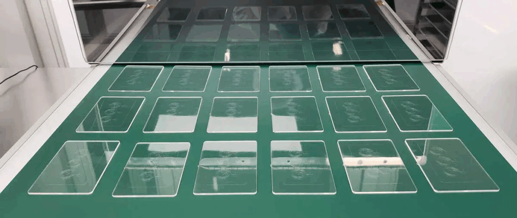
High volume PDMS device fabrication at DBM Medix (image courtesy of and © DBM Medix, 2025)

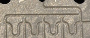
I recently had the privilege of chatting with Anuthasan Balasingam at DBM Medix (Montréal, Canada) about their LiQon™ microfluidics manufacturing process. In short, LiQon™ allows microfluidic devices to be injection moulded directly from a silicon master, which is kind of revolutionary! A photo from DBM Medix of injection moulded polydimethyl siloxane (PDMS) devices manufactured at volume at their facility is shown at right. In the next 2-3 paragraphs I’ll try to provide the context to understand why this is, so if you already understand how microfluidic devices are made out of glass, silicon, as well as hard and soft plastics, you might want to skim or skip ahead. 🙂

How are microfluidic devices made, and from what? Well, it depends; there are quite a variety of ways to make microfluidic devices, but the mainstream approaches that lend themselves well to manufacturing are few indeed. Historically, starting in the 1970s, microfluidic devices were made in glass and silicon using photolithographic processes that were ported over from the semiconductor sector, and that are also used to manufacture MEMS (microelectromechanical systems) devices. Glass and silicon microfluidic device manufacturers include Teledyne MEMS (formerly Micralyne and Dalsa; both in Canada), Micronit (the Netherlands) and Atomica (formerly IMT; USA). In the 1990s, polymer microfluidic prototyping became popular, leading to manufacturing of devices in hard thermoplastics (e.g. polymethyl methacrylate (PMMA), polycarbonate (PC), cyclic olefin polymers and copolymers (COP & COC)) as well as in softer elastomers (e.g. polydimethylsiloxane (PDMS), a silicone rubber). Thermoplastic manufacturers include microfluidic ChipShop (Germany), ThinXXS (Germany), Schott MiniFAB (Australia), while elastomer manufactuers include DBM Medix, HiComp (USA/China), and applications company Standard BioTools (formerly Fluidigm; USA) gets an honourable mention as an applications pioneer in elastomer devices. In some cases, thermoplastics and/or elastomers can be used to make devices through lamination; manufacturers include ALine and MicroMed Solutions (both USA).

PDMS, and every other device material, has particular chemical and physical properties that may make it preferable for a given application, and non-viable for another. In addition, manufacturing capabilities have evolved for all three types of materials (i.e. glass & silicon, thermoplastics, and elastomers), allowing for cost-effective production of launched microfluidic products made from each. In the end, the application’s business and technical requirements dictate the material types and manufacturing processes that are best suited.

Focussing on PDMS for a moment, it is soft and porous (for better or worse, depending on the application), relatively clear in the visible spectrum (~90% transmission from the near IR to the near UV for a 3 mm thick sample, according to a 2019 Heliyon paper from the González-García group), and can be replicated from its cast or mould master with high fidelity, including at micrometer scales, to yield optically smooth devices. Biocompatibility ranges from excellent to unsatisfactory, depending on the application. PDMS has become very popular for device prototyping over the last 20 years largely because a negative mould master can be created relatively easily from silicon, glass, metal or other material, and then the unreacted PDMS can be cast in the mould to create the positive device form, complete with microfluidic channels, chambers, etc. While very convenient for small volume production of 10s or 100s of devices, PDMS casting is not amenable to high volume manufacturing, so the majority of launched microfluidic products have been made from injection-moulded thermoplastics and/or photolithographically patterned glass and silicon, both proven high throughput, cost-effective manufacturing methods. Even if PDMS is a viable or preferred material for a given microfluidic application, it is usually left behind due manufacturing hurdles, such as its slow curing time (Dow’s SYLGARD™ 184 Silicone Elastomer (PDMS) requires 48 h to cure at room temperature, down to 10 min at 150°C), and possible need for chemical release agents to free the material from the mould.

Now, back to DBM Medix! So, what’s the big deal with their LiQon™ process for PDMS prototyping and manufacturing? It directly addresses several of the major manufacturing issues mentioned above.

  1. Devices are made directly from silicon masters, so a) the same process for creating mould masters can be used, and b) the high fidelity fabrication of micro-features possible with a silicon master persists.
  2. The proprietary LiQon™ process is truly injection moulding, not casting, so all the high volume manufacturing benefits of this established process apply. For example: a) shot times are short, on the order of 30 s; b) investments for both prototyping and manufacturing are low; and c) automated production and assembly are in place, so reaching high microfluidic device quality and consistency at an economical pricepoint is attainable.
  3. Mould release agents are not required, so concerns about contamination and biocompatibility of these agents are obviated.
  4. Prototyping turn-around times are pretty fast, around 1-3 weeks.
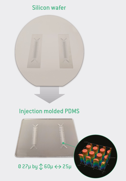
DBM Medix’s LiQon™ fabrication process using injection moulding starting from a silicon master (image courtesy of and © DBM Medix, 2025)

An image from DBM Medix’s LiQon™ info sheet, at right, is helpful, showing the fabrication of some 27 µm pillars (diameter x height x on-centre pitch = 27 x 60 x 50 µm). Above is the silicon wafer with the negative microfabricated pillar array (cylindrical cavities instead of solid pillars), and the injection moulded PDMS device created from it, with the pillars as positive features. A circular close up image is a scanning electron micrograph (SEM) showing the pillars up close, and demonstrating the smooth replication and clean release of these features.

Check out DBM Medix’s recent blog post on PDMS injection moulding via their LiQon™ process for more information, and to get in touch with them directly.

If you think that PDMS could be the right material for your microfluidic/microfabricated device or concept, or if you’re not sure what material would be best, drop me a line. I’m agnostic with regard to the material or method, except that I strive to guide my client towards the materials and fabrication processes that are best suited for their application and business needs. If, after discussing your application in detail, PDMS looks like the winner or a contender, we can contact DBM Medix together to explore what doing your prototyping and manufacturing with them might look like.

Survey: metrology in microfluidics

Survey: metrology in microfluidics

The Microfluidics Association is participating in a workshop on November 13th-14th, 2023 focussed on on metrology in microfluidics, and hosted by the metrology wing of the French Cetiat institution. In preparation, we at the Microfluidics Association (I’m on the Board) want to brush up on what the microfluidics community wants and needs as regards metrology. Here’s a letter from Henne van Heeren, fellow board member.


“For our work in developing standards and metrology protocols it is crucial that we know what the community needs. Therefor you you are invited to participate in our survey concerning prioritizing metrology and standardization work for the coming years.
Your participation in this study is completely voluntary, so if you feel uncomfortable answering any questions, you can skip questions or withdraw from the survey at any point.
The information you will supply will be coded and will remain strictly confidential.

Thank you very much for your time and support. Please start with the survey now by clicking on https://www.surveymonkey.com/r/D6RF9JM

This survey is held in preparation for the November workshop “on the road to standardization in microfluidics and organ-on-chip”. For more information on this workshop, please click here.

Best regards on behalf of the Microfluidics Association

Henne van Heeren
henne@enablingMNT.com
0031 78 6300748

Download our published whitepapers: https://microfluidics-association.org

We acknowledge the support of the MFMET project, https://mfmet.eu/ and the European Metrology Programme for Innovation and Research: EMPIR.”


On behalf of the Microfluidics Association, I would like to encourage any and all working in microfluidics to provide your input about metrology via our survey. I gave my 2¢ this morning! 🙂

Zeon acquires Edge Precision Manufacturing

Zeon acquires Edge Precision Manufacturing

According to recent LinkedIn posts and a press release, polymer manufacturing leader Zeon Specialty Materials Inc. (subsidiary of Zeon Corporation, Japan) recently acquired Edge Precision Manufacturing, a microfabrication manufacturing house based in the Boston, MA area. In the world of microfluidics, Zeon is a well known manufacturer of its cyclic olefin copolymers (COPs) Zeonor® and Zeonex®, widely used in the injection moulding of microfluidic products.

The manufacture of plastic microfluidic devices is most often performed with injection moulding, given its economic edge at high volumes, and less often with hot embossing, given its slower throughput, however hot embossing has the edge for devices with more demanding fine features and fidelity requirements. Edge Precision Manufacturing, formerly Edge Embossing, is able to combine the best of both worlds with a high volume, high precision hybrid approach, where hot embossing is used for the most demanding areas of a component, and injection moulding for the more routine feature sizes.

Zeon’s acquisition of Edge Precision Manufacturing is the latest in a series of microfluidics and MEMS fab house acquisitions that has seen Invenios acquired by Corning and thinXXS acquired by IDEX in 2017, miniFAB acquired by Schott and Micralyne acquired by Teledyne in 2019, and most recently microLIQUID acquired by TE Connectivity in 2021.

908 Devices: an investment opportunity?

908 Devices: an investment opportunity?

In a recent Forbes profile, author Peter Cohan suggests that 908 Devices, based in Boston, may be a good company to consider for investment. He notes that they are doing several things right that are keeping them nimble, including attracting top talent, empowering employees closest to clients, launching products quickly and fighting bureaucracy.

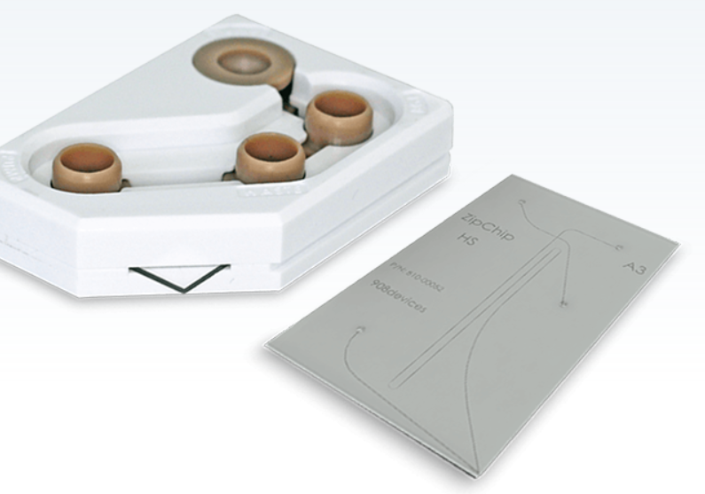
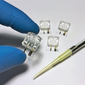
Zip Chip ESI microfluidic device.
Copyright: 908 Devices

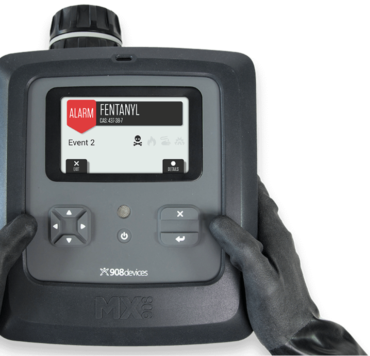
The company uses microfluidic chips for electrophoresis-based sample preparation and electrospray ionisation (ESI) for sample introduction into their revolutionary desktop or hand-held, low power, high (atmospheric) pressure mass spectrometers (HPMS) that perform the sample analysis. In some cases the HPMS operates alone. More information is available on their website, including a listing of their suite of patents relating to both the microfluidic ESI and HPMS aspects of their core technology. Applications vary from cell biology analysis, detection of drugs (e.g. fentanyls, opioids and amphetamines), explosives and chemical warfare agents. Importantly, the chips are easy to use, and instrumentation is coupled to powerful electronics and software to automate all operations and analysis computations, and thus afford a simplified, practical interface suitable for a broad base of operators.

MX 908 system. Copyright: 908 Devices

The company was founded 9 years ago, and had its IPO in December, 2020. It’s stock has dipped slightly, but revenue grew by 50% last year to USD $26.9 M and is projected to grow another 45% in 2021. The company also just landed a USD $25M purchase contract from the US Army for 350 of its MX908® portable MS instruments for on-site explosive threat detection and evaluation applications.

Cohan notes that 908 Devices avoids agility potholes such as forcing valuable employees who intimately understand the technology, customers and competition to do “tooth-cleaning-like reviews” for C-suite executives. CEO Kevin Knopp noted in his interview with Cohan that they intentionally maintain a fairly flat organisational structure, hire high-calibre talent, and empower their employees to listen to customers and react accordingly.

Cohan summarises: “If 908 can figure out an easy button for sustaining 50% annual revenue growth, its stock is a buy.”

On-demand microfluidic devices in Petri dish

On-demand microfluidic devices in Petri dish

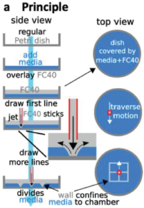
principleNew research from Edmond Walsh’s group at the University of Oxford and Iota Sciences demonstrates rapid in situ device prototyping in a plastic Petri dish using robotic jet printing.  The work was published in Advanced Science 2 weeks ago.

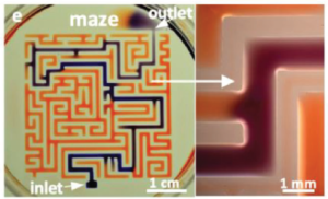
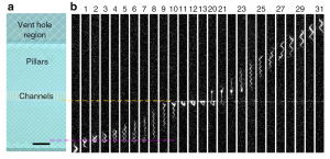
Beginning with a Petri dish containing an aqueous cell medium, the procedure entails covering the medium with a second immiscible layer of FC40 fluorocarbon, and then jetting the fluorocarbon through the medium to make contact with and stick to the Petri dish via preferential wetting.  The moving jet nozzle can thus define channel & chamber walls bonded to the Petri dish surface and directly write a fluidic channel network according to a CAD layout input.  The jet stays in the fluorocarbon, making the fabrication contactless.  Writing time depends on the design complexity, but may be about five minutes.  A diagram of the fabrication procedure is shown at right above, and a fluidic maze structure created with this technique is show at right below.  First author Cristian Soitu’s Twitter feed (@CristianSoitu) has an impressive video showing the creation of some devices.

mazeThe authors have done a nice job of characterising the various parameters relevant to creating walls or features from the fluorocarbon, such as jet nozzle height, diameter, flow rate, lateral speed, wall thickness and channel widths.  The ability to pipet into enclosed chamber arrays was also explored in terms of volume ranges and resistance to cross-contamination.  Preliminary cloning studies with different cells suggested comparable cloning efficiency vs. normal Petri dishes without fluorocarbon structures.
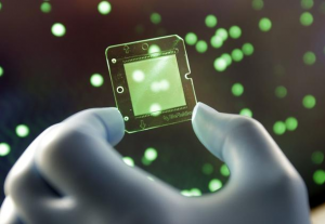
The possibilities afforded by such a direct-write technique are compelling.  An ability to create custom microfluidic structures for a given pattern of cells or conceivably other analytes adsorbed on a solid substrate with secluded, sterile and controllable environments seems like a window into new analytical techniques enabled by powerful sampling and work-up strategies.  Iota Sciences appears to be moving the technology forward for cell cloning purposes.

BioFluidica’s microfluidic tumour detection technology

BioFluidica’s microfluidic tumour detection technology

biofluidica-deviceA recent article by Bradley Fikes in the San Diego Union-Tribune highlighted the progress achieved by a local leading biotech company, BioFluidica.  Founded by Professor Steve Soper at Kansas University and headed up by CEO Dr. Rolf Muller, two veterans in the area of microfluidics research and product development, the company is effectively translating the inherent capabilities of lab-on-a-chip technology into the foundation of their cancer-screening products.

BioFluidica uses injection moulding to economically mass produce their plastic microfluidics chips.  While injection moulding has been effectively applied to microfluidic products with ‘normal’ channel geometries (width similar to depth), BioFluidica’s device channels appear to be tall and thin, making high fidelity, high volume reproduction challenging.  That they can use injection moulding for these devices is no mean feat; it is not a surprise to hear that they had to go through several manufacturers before finding one in Austria equal to the task

The devices are used to perform affinity-based assays of circulating tumour cells (CTCs), and work directly with whole blood, a distinct advantage in terms of cost and ease-of use, and also likely in terms of the quality of the assay results.  BioFluidica estimates that lung biopsy screens would be reduced from $10,000 USD to roughly $5,000 using their technology.

HJC Consulting Product Profile Award

HJC Consulting Product Profile Award

HJC Consulting is pleased to launch a newd90_dsc_0575-cu monthly Product Profile Award series to help give microfluidic product developers a leg up in creating awareness about current or upcoming products. The award will provide that month’s successful applicant a chance to get the word out through a product on HJC Consulting’s website and social media channels regarding their microfluidic or lab-on-a-chip product’s milestones such as a launch, revision with enhanced performance, new product research or patent publication, etc.

The profile will be awarded, free of charge, to one submission per month.  To be eligible, a profile submission must:

  • speak to the technical method of operation and capabilities of the product;
  • include imagery (photos, data, logo, etc.) for which copyright is owned;
  • be free of copyrighted, confidential or proprietary information;
  • highlight preferred applications and/or targeted market segments;
  • include details concerning:
    • (co-) developer & (co-) author email addresses, and social media addresses if desired;
    • company physical address, contact & phone number, website & media release URLs, social media addresses for Facebook, Twitter and LinkedIn; and
  • be 300 words or less.

See examples of current blog posts for guidance.

The profile will be hosted on the HJC Consulting blog, and will be posted simultaneously through HJC Consulting’s social media accounts.  Suggestions for social media post content is also welcomed.

Please send queries or submissions via email to John Crabtree.  Successful submissions may be edited for content and length by HJC Consulting.  Unsuccessful submissions may be considered for subsequent months, if desired.

We hope to see your application soon!

Bullish microfluidics market projections by MarketsandMarkets

Bullish microfluidics market projections by MarketsandMarkets

A recent report by Markets and Markets cited in an article by The Health Star shows aggressive microfluidics product market growth predictions that exceed previous strong predictions from other research enterprises.

Markets and Markets put the 2017 market value at $8.28 B USD with a compound annual growth rate (CAGR) of 22.6% forecasted until 2023.  Other research firms, however, have lower estimates of both the current market as well growth predictions for similar time spans.  Yole Dévelopment’s 2017 report, for example, estimated the 2016 market to be ~$2.1 B USD, and projected a CAGR of 18% out to 2022.  A 2017 report by Transparency Market Research put the 2016 market at $4.76 B USD and CAGR at 11.4% through 2025.  Future Market Insights’ 2017 report on the point-of-care (PoC) segment of the microfluidics market, the largest segment in their view, estimates this segment to have been $1.0 B USD in 2016, and to grow at a 14.5% CAGR until 2026.

The reason for the large differences between Markets and Markets’ estimates and those of others – roughly, 2-4x larger market values and 1.25-2x larger CAGRs – is not clear, but may be due to definition of the market scope, i.e. what products are considered “microfluidic”.

Nanofluidic DNA sieving device from IBM

Nanofluidic DNA sieving device from IBM

nf-dna-reptationFascinating research from the Qinghuang Lin lab at IBM Research in NY, published in Nature Communications and highlighted in Cytofluidix, shows an elaborate but potentially mass-producible microfluidic and nanofluidic lab-on-a-chip device that draws DNA molecules through arrays of nanometre-sized pillars.  The DNA reptation in these structure stretches the molecules out, as in gel-based electrophoretic separations of DNA, and may enable identification of biomarkers that indicate diseases.  The Cytofluidix summary page shows an engaging video of DNA migration through the pillar array.

The research team had to overcome sizable challenges associated with the nanofabrication of the different structures that act as the DNA sieving medium.  Researchers used a sacrificial silicon layer for the nanofluidic channels, and were able to overcome diffusion-limitted etching constraints by using temporary venting holes to accelerate the etching by 2 orders of magnitude.  This process improvement may be the key to making the device a manufacturable product instead of a clever academic exercise.

Microfluidic nanoparticle analysis by Spectrodyne

Microfluidic nanoparticle analysis by Spectrodyne

spectradyne-uf-coulter-counter-deviceA recent article by Azo Materials featured a microfluidic nanoparticle analyser product from Spectrodyne.  The “nCS1” system appears to reap the benefits of precise small volume fluid manipulations in disposable microfluidic cartridges to eliminate sample cross-talk and any need for cleaning.

The system is an advanced Coulter counter, and has sufficiently high resolution to allow it to achieve superior measurements of particle polydispersity in a given sample.  Particle sizing is from 40-2000 nm for 10^5 to 10^12 particles/mL, with precision of better than +/- 3% on sizing and +/-10% on concentration.

Micro-sized gaskets from PPE

Micro-sized gaskets from PPE

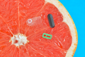
ppe-grapefruit-gasketsInterfacing with users and the real world is one of the many practical challenges facing any team engaged in technology-based product development.  For microfluidics or lab-on-a-chip based products, this is nears the top of the list of challenges to be addressed early, starting at the duct tape/super-glue prototyping phases through to product launch.  Interfaces need to be small, snug and low dead volume to reap the benefits of the miniaturised operations going on inside the microfluidic network.

To this end, I thought I’d highlight what appears to be a convenient product offering from Precision Polymer Engineering.  They seem to have very nicely crafted, very small elastomer components that might obviate the need to a) press the guy with the steadiest hand in the lab into service to cut Teflon gaskets, b) source those parts at volume once designs are frozen, etc.  See image above from their recent tweet.  They’ve produced a brochure that shows different elastomers, dimensions and standard parts on offer (gaskets, ferrules, o-rings, etc.).

Metafluidics – open microfluidics repository

Metafluidics – open microfluidics repository

Open-source tools, parts, methods, systems, and data for synthetic biology and community-driven repositories where they can be shared.I just read a Cytofluidix article that described an interesting new site, Metafluidics, that is acting as an open-source repository of designs and information for the microfluidics community.  It’s free, and users can browse submitted designs, view blog posts where other users comment on designs, and download a design CAD file to be able to reproduce a device.

The repository was built at MIT’s Lincoln Laboratory, and is maintained by their Media Lab.  Metafluidics’ director, David Kong, highlights that this will hopefully accelerate the diffusion of microfluidic technology and reduce the amount of “reinventing the wheel” in the field.  Currently, different researchers working in a given microfluidic field often cannot use other published research as a stepping stone to move their own research forward, as previous work may have limitted details included in the journal publications.

See the Metafluidics website, Cytofluidix article or Kong’s recent Nature Biotechnology article for more information.

Micronit’s microfluidic prototyping service, Miproto

Micronit’s microfluidic prototyping service, Miproto

Miproto logoMicronit, a Dutch fab house that has been engaged in microfluidics for over a decade, has a new and very user-friendly à la carte prototyping service for the microfluidics research and product development community called Miproto.

A prospective customer need only define the basics of their device, i.e. material type, basic processing on each substrate, size of devices & number required, and a price vs. quantity table quote is produced.  I should be specific: produced in seconds, à la build-your-own-car webpages offered by most auto makers.  A simple 2 substrate, single glass etch pattern design I entered with access holes and 1″ x 1″ devices generated a quote of €4792 for 18 devices delivered with a 3-week turn-around.  That’s pretty good!

Microfluidics market projections by FMI

Microfluidics market projections by FMI

Interesting summary of new microfluidics market report from Future Market Insights projects robust growth for next decade. PoC testing is expected to account for 33% of revenues.

Contrasting somewhat with other reports, ceramics are said to be the dominant material of choice: “Ceramics segment is expected to remain dominance, accounting for over 42% market value share in 2026, followed by glass, polymer, and silicon.”