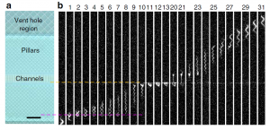
 Researchers from the Mace lab at Tufts University recently published an article in Scientific Reports highlighting their new open-source CAD software that is tailored for the design of paper microfluidic devices. The software works across all OS platforms, appears fairly straightforward and user-friendly, and likely capable of covering most of the normal aspects of geometrical design for channel networks, based on examples presented.
The software is provided by the authors gratis in a laudable effort to reduce the costs associated with chip design, especially for resource-constrained environments such as schools and labs in developing countries. The price for subscription or purchase of industry-standard CAD software can be prohibitive, easily reaching tens of thousands of dollars, and scaling with the number of users, etc. Removing the cost of design SW breaks down a significant cost barrier to innovation for paper microfluidics, a technology that otherwise boasts very economical costs for consumable materials (paper) and fabrication (wax printing with commercially available printers).