Open-source CAD for paper microfluidics

Open-source CAD for paper microfluidics

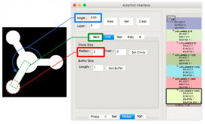
autopadResearchers from the Mace lab at Tufts University recently published an article in Scientific Reports highlighting their new open-source CAD software that is tailored for the design of paper microfluidic devices.  The software works across all OS platforms, appears fairly straightforward and user-friendly, and likely capable of covering most of the normal aspects of geometrical design for channel networks, based on examples presented.

The software is provided by the authors gratis in a laudable effort to reduce the costs associated with chip design, especially for resource-constrained environments such as schools and labs in developing countries.  The price for subscription or purchase of industry-standard CAD software can be prohibitive, easily reaching tens of thousands of dollars, and scaling with the number of users, etc.  Removing the cost of design SW breaks down a significant cost barrier to innovation for paper microfluidics, a technology that otherwise boasts very economical costs for consumable materials (paper) and fabrication (wax printing with commercially available printers).

Nanofluidic DNA sieving device from IBM

Nanofluidic DNA sieving device from IBM

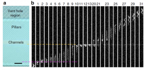
nf-dna-reptationFascinating research from the Qinghuang Lin lab at IBM Research in NY, published in Nature Communications and highlighted in Cytofluidix, shows an elaborate but potentially mass-producible microfluidic and nanofluidic lab-on-a-chip device that draws DNA molecules through arrays of nanometre-sized pillars.  The DNA reptation in these structure stretches the molecules out, as in gel-based electrophoretic separations of DNA, and may enable identification of biomarkers that indicate diseases.  The Cytofluidix summary page shows an engaging video of DNA migration through the pillar array.

The research team had to overcome sizable challenges associated with the nanofabrication of the different structures that act as the DNA sieving medium.  Researchers used a sacrificial silicon layer for the nanofluidic channels, and were able to overcome diffusion-limitted etching constraints by using temporary venting holes to accelerate the etching by 2 orders of magnitude.  This process improvement may be the key to making the device a manufacturable product instead of a clever academic exercise.

Origami switches for paper microfluidics

Origami switches for paper microfluidics

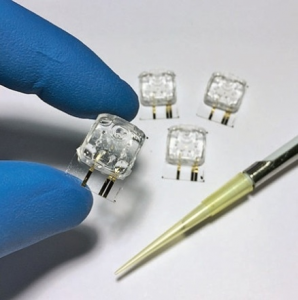
Research from Santosh Pandey‘s lab at Iowa State U, published in Lab on a Chip and highlighted in Cytofluidix, shows actuation of paper microfluidics switches/valves with effective, fast performance.  Several different configurations were demonstrated, including single-pole-single-throw (normally open and normally closed), single-pole-double-throw, by analogy to electrical switch terminology.  The switches appear to actuate in seconds, which is suitable for many paper microfluidics applications.  A video of the switches in action can be viewed on YouTube.

Several key advantages come to mind with this advance.  Paper microfluidics has simplicity, low cost manufacture and portability amongst its key attributes, but these are less credible if the devices also require expensive, power-intensive peripheral hardware for e.g. fluid movement, valve actuation, detector operation, communications, etc.  Implementation of this technology in a commercial product might reduce or eliminate the need for expensive pumps and valves (and accompanying electrical power consumption) for fluid flow and valving on a device.  This could enable very low cost analysis applications targeting harsh or remote environments.

Microfluidic nanoparticle analysis by Spectrodyne

Microfluidic nanoparticle analysis by Spectrodyne

spectradyne-uf-coulter-counter-deviceA recent article by Azo Materials featured a microfluidic nanoparticle analyser product from Spectrodyne.  The “nCS1” system appears to reap the benefits of precise small volume fluid manipulations in disposable microfluidic cartridges to eliminate sample cross-talk and any need for cleaning.

The system is an advanced Coulter counter, and has sufficiently high resolution to allow it to achieve superior measurements of particle polydispersity in a given sample.  Particle sizing is from 40-2000 nm for 10^5 to 10^12 particles/mL, with precision of better than +/- 3% on sizing and +/-10% on concentration.

Micro-sized gaskets from PPE

Micro-sized gaskets from PPE

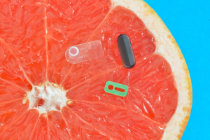
ppe-grapefruit-gasketsInterfacing with users and the real world is one of the many practical challenges facing any team engaged in technology-based product development.  For microfluidics or lab-on-a-chip based products, this is nears the top of the list of challenges to be addressed early, starting at the duct tape/super-glue prototyping phases through to product launch.  Interfaces need to be small, snug and low dead volume to reap the benefits of the miniaturised operations going on inside the microfluidic network.

To this end, I thought I’d highlight what appears to be a convenient product offering from Precision Polymer Engineering.  They seem to have very nicely crafted, very small elastomer components that might obviate the need to a) press the guy with the steadiest hand in the lab into service to cut Teflon gaskets, b) source those parts at volume once designs are frozen, etc.  See image above from their recent tweet.  They’ve produced a brochure that shows different elastomers, dimensions and standard parts on offer (gaskets, ferrules, o-rings, etc.).

Degradable substrate materials for microfluidic devices

Degradable substrate materials for microfluidic devices

3-D-printed Biomaterials That Degrade On Demand DevelopedNew research from Ian Wong‘s group at Brown University published in Lab on a Chip and featured in a Technology Networks article shows 3-D printed microfluidic devices with on-demand degradation of substrate materials.  Not only does this allow for easy fabrication of complex structures, but also allows for them to be controllably modified ‘on the fly’.  The key is in the use of reversibly photopolymerisable hydrogels with ionic cross-linkers.  Cross-linkers can then be removed with chelating agents.  The stiffness and degradation kinetics are controllable by the choice of metal cation for the ionic cross-linker.  Both the sodium alginate ionic cross-linking polymer and chelating agents chosen appear to be biocompatible with the human mammary cells used in the study.

While normally used to directly create the microfluidic structures, the reversible gels were also used in a second approach to create complex moulds that are removed after a second polymer forms around the reversible gel.

The technology may potentially be applied as an adaptive or stimulus responsive material for use in sensing, actuation, drug delivery, cell migration monitoring for wounds or cancer, artificial tissue scaffolding or other applications.

Improved ultrasonic welding for microfluidic device bonding

Improved ultrasonic welding for microfluidic device bonding

An interesting  Cytofluidix post highlights recent work by a collaborative team of researchers at both Singapore’s A*STAR’s SIMTech facility and Nanyang Technological University, and at the Seoul National University of Science and Technology, based on their article published in the Journal of Materials Processing Technology.

The focus is on addressing the drawbacks encountered with ultrasonic welding as a bonding technique for plastic microfluidic devices.  Ultrasonic welding is attractive because it lends itself to batch processing of microfluidic devices, and employs relatively established, inexpensive and compact equipment.  As currently used, however, ultrasonic welding is often not up to the task, from a quality perspective, since uneven energy distribution may distort or melt the microfabricated structures, and air bubbles may also be incorporated.

According to Gary Sum Huan Ng from the SIMTech group, the team’s innovation is to introduce a sandwiched composite film between the two polymer substrates that are to be bonded.  The film contains PMMA microspheres within a PDMS matrix, and the microspheres melt during ultrasonic welding, and prevent bubble formation and substrate material flow.

Metafluidics – open microfluidics repository

Metafluidics – open microfluidics repository

Open-source tools, parts, methods, systems, and data for synthetic biology and community-driven repositories where they can be shared.I just read a Cytofluidix article that described an interesting new site, Metafluidics, that is acting as an open-source repository of designs and information for the microfluidics community.  It’s free, and users can browse submitted designs, view blog posts where other users comment on designs, and download a design CAD file to be able to reproduce a device.

The repository was built at MIT’s Lincoln Laboratory, and is maintained by their Media Lab.  Metafluidics’ director, David Kong, highlights that this will hopefully accelerate the diffusion of microfluidic technology and reduce the amount of “reinventing the wheel” in the field.  Currently, different researchers working in a given microfluidic field often cannot use other published research as a stepping stone to move their own research forward, as previous work may have limitted details included in the journal publications.

See the Metafluidics website, Cytofluidix article or Kong’s recent Nature Biotechnology article for more information.

Micronit’s microfluidic prototyping service, Miproto

Micronit’s microfluidic prototyping service, Miproto

Miproto logoMicronit, a Dutch fab house that has been engaged in microfluidics for over a decade, has a new and very user-friendly à la carte prototyping service for the microfluidics research and product development community called Miproto.

A prospective customer need only define the basics of their device, i.e. material type, basic processing on each substrate, size of devices & number required, and a price vs. quantity table quote is produced.  I should be specific: produced in seconds, à la build-your-own-car webpages offered by most auto makers.  A simple 2 substrate, single glass etch pattern design I entered with access holes and 1″ x 1″ devices generated a quote of €4792 for 18 devices delivered with a 3-week turn-around.  That’s pretty good!

Heart-on-a-chip research from LLNL

Heart-on-a-chip research from LLNL

iChipNew research from Lawrence Livermore National Laboratory and Harvard Medical School, published in Lab on a Chip, shows a microfabricated cardiac sensing platform that can monitor tissue adhesion, electrophysiology and contractility on a single device.  It’s used to test the effectiveness of new cardiac drugs.  Human heart cells are grown on the electrode-array chip, and then their cellular beating is tracked via electrical signals sensed by the interdigitated electrodes.

The use of such devices could yield significant advantages for cardiac drug development by signalling problems with a given drug candidate early in the process, long before clinical trials.  The technology may also obviate the need for animal testing.

Microfluidic dewatering for sustainable farming

Microfluidic dewatering for sustainable farming

uFraction8Very interesting technology from µFraction8 based at Heriot Watt University in Scotland may help address sustainable farming approaches for food, animal feed and pharmaceuticals bioproduction.  Sustainable approaches can use 20x less land area.  Post bioreactor dewatering comprises ~40% of the cost of bioproduction; µFraction8’s microfluidic devices can potentially reduce the cost of dewatering by 75%, which would have a dramatic impact on viability.  See Akzo Nobel article for more details.


Welcome to our new website!

Welcome to our new website!

hjc-consulting-logoIf you’ve visited HJC Consulting’s website before, please explore anew!  You’ll notice that it has changed significantly … and hopefully very much for the better!  We’ve tried to expand on what we offer and how we operate to give you a better idea of how you might be able to use us to further your project objectives.

We believe we’ve patched a bug that, when you scrolled down, created a large grey box blocking the page.  This affected iPads using Firefox, Chrome and Safari, and Apple laptop and desktop computers using Safari.  Please feel free to e-mail us if you see this or any other issue crop up; we want to ensure everything is working smoothly.

Notice to web log (blog) reader

Notice to web log (blog) reader

Welcome!  I hope you find some of the business and technology posts here to be of interest.

After April, 2017, blog posts reflect the time at which the information was originally posted, often simultaneously on Facebook, Twitter and LinkedIn.  A major revision to the HJC Consulting website was pushed through in April, 2017, and reflects the creation of the blog; at that time, I ‘reposted’ several of HJC Consulting’s LinkedIn and Twitter posts with approximate dates from the last couple years here just for reference purposes.

Also, I’m happy to entertain requests to post articles on your microfluidic research or products; please send me an email if you’re interested.

Enjoy!

Microfluidics market projections by FMI

Microfluidics market projections by FMI

Interesting summary of new microfluidics market report from Future Market Insights projects robust growth for next decade. PoC testing is expected to account for 33% of revenues.

Contrasting somewhat with other reports, ceramics are said to be the dominant material of choice: “Ceramics segment is expected to remain dominance, accounting for over 42% market value share in 2026, followed by glass, polymer, and silicon.”